Sequential circuits are circuits whose output at any instant of time depends on all previous inputs.
Flip flops are sequential circuits which are configured using a set of logic gates and they can be used as a memory element. A logic gate by itself has no storage capacity but several logic gates connected together can permit storage of data.
Flip flops are also called as bistable multivibrators.
Flip-flops can be either simple (transparent or opaque) or clocked
(synchronous or edge-triggered). Although the term flip-flop has
historically referred generically to both simple and clocked circuits,
in modern usage it is common to reserve the term flip-flop exclusively for discussing clocked circuits; the simple ones are commonly called latches.
1 latch:
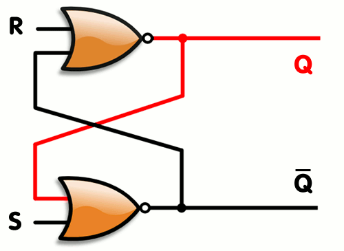
an active high SR latch

timing diagram of a simple SR latch
2.gated latches:
gated SR latch:
Tt is sometimes useful in logic circuits to have a multivibrator which
changes state only when certain conditions are met, regardless of its S
and R input states. The conditional input is called the enable, and is symbolized by the letter E.
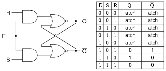
When the E=0, the outputs of the two AND gates are forced to 0,
regardless of the states of either S or R. Consequently, the circuit
behaves as though S and R were both 0, latching the Q and not-Q outputs
in their last states. Only when the enable input is activated (1) will
the latch respond to the S and R inputs
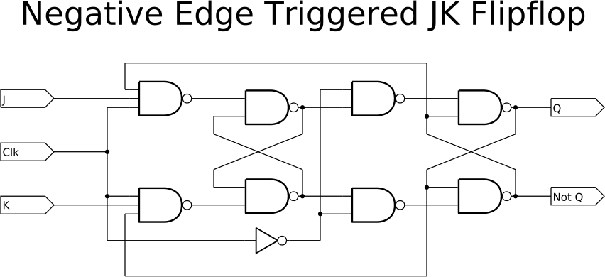
3.edge triggered flip flop:
One method of enabling a multivibrator circuit is called edge triggering, where the circuit’s data inputs have control only during the time that the enable input is transitioning from one state to another.
edge triggered SR flip flop:
Edge-triggered S-R flip-flop
The basic operation is illustrated below, along with the truth table for this type of flip-flop. The operation and truth table for a negative edge-triggered flip-flop are the same as those for a positive except that the falling edge of the clock pulse is the triggering edge.
 |
 |
| As S = 1, R = 0. Flip-flop SETS on the rising clock edge. |
Note that the S and R inputs can be changed at any time when the clock input is LOW or HIGH (except for a very short interval around the triggering transition of the clock) without affecting the output. This is illustrated in the timing diagram below:

Edge-triggered J-K flip-flop
The J-K flip-flop works very similar to S-R flip-flop. The only difference is that this flip-flop has NO invalid state. The outputs toggle (change to the opposite state) when both J and K inputs are HIGH. The truth table is shown below.

Edge-triggered D flip-flop
The operations of a D flip-flop is much more simpler. It has only one input addition to the clock. It is very useful when a single data bit (0 or 1) is to be stored. If there is a HIGH on the D input when a clock pulse is applied, the flip-flop SETs and stores a 1. If there is a LOW on the D input when a clock pulse is applied, the flip-flop RESETs and stores a 0. The truth table below summarize the operations of the positive edge-triggered D flip-flop. As before, the negative edge-triggered flip-flop works the same except that the falling edge of the clock pulse is the triggering edge.


Applications of filp-flops:
Flip-flops have wide and extensive application in semiconductor memories,counters,shift and storage registers.
They can also be used for binary addition,serial decode,comparison and timing function.
No comments:
Post a Comment