Various logical operations can be performed by interconnection of the appropriate logic elements.
We will be seeing the most commonly used combinational circuits in this chapter.
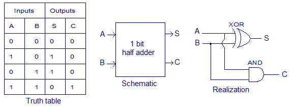
1.HALF ADDER:
An adder is a combinational circuit which adds two input numbers to give a sum and a carry element.
Adders are used to add either binary numbers ,x-s 3 code etc.
A half adder is a combinational arithmetic circuit which adds two numbers and give a sum bit and a carry bit.
If A and B are the input bits, then sum bit (S) is the X-OR of A and B
and the carry bit (C) will be the AND of A and B. From this it is clear
that a half adder circuit can be easily constructed using one X-OR gate
and one AND gate.
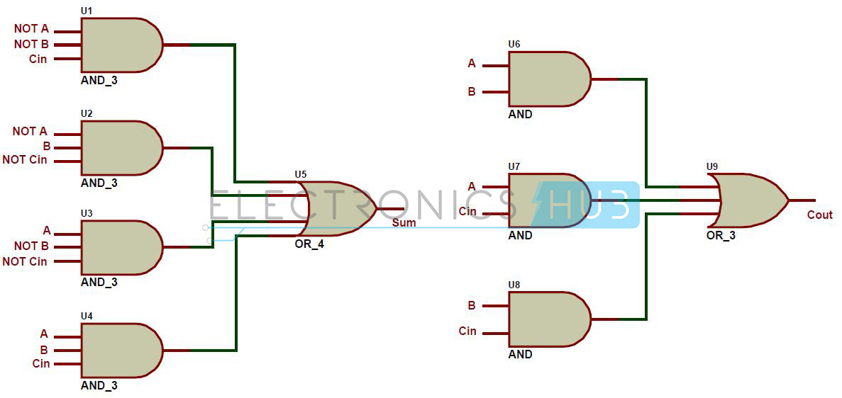
2. Full adder:
A full adder is an arithmetic circuit that adds two bits and a carry and outputs a sum bit and a carry bit.

Even though a full adder can be constructed using only two half adders,the disadvantage is that the bits must pass through several gates in succession which makes the propagation delay greater than the configuration using AOI logic implementation.Below given is the implementation of full adder using AOI logic.
3.Half subtractor:
A subtractor is an arithmetic circuit used for subtracting the LSB of the subtrahend from the LSB of the minuend.When subtraction is performed the output is a difference bit and a borrow bit.


For consideration of borrow element from a previous subtraction the full subtractor circuit mentioned below is used.
4.Full subtractor:
The full subtractor is a combinational circuit which is used to perform subtraction of three input bits: the minuend  , subtrahend
  , and borrow in
  . The full subtractor generates two output bits: the difference
  and borrow out
  .
.
, subtrahend , and borrow in . The full subtractor generates two output bits: the difference and borrow out .
Full subtractor logic diagram:
The full subtractor circuit can also be realised using universal gates that is using only nand and nor gates.
5.Look ahead carry adder:
A carry-lookahead adder (CLA) or fast adder is a type of adder used in digital logic.
A carry-lookahead adder improves speed by reducing the amount of time
required to determine carry bits. It can be contrasted with the simpler,
but usually slower, ripple carry adder
for which the carry bit is calculated alongside the sum bit, and each
bit must wait until the previous carry has been calculated to begin
calculating its own result and carry bits (see adder
for detail on ripple carry adders). The carry-lookahead adder
calculates one or more carry bits before the sum, which reduces the wait
time to calculate the result of the larger value bits.
To reduce the computation time, there are faster ways to add two binary numbers
by using carry lookahead adders. They work by creating two signals P and G known to be
Carry Propagator and Carry Generator. The carry propagator is
propagated to the next level whereas the carry generator is used to generate the output carry
,regardless of input carry. The block diagram of a 4-bit Carry Lookahead Adder is shown here below -

The corresponding boolean expressions are given here to construct a carry lookahead adder.
In the carry-lookahead circuit we ned to generate the two signals carry propagator(P) and carry generator(G),
Pi = Ai ⊕ Bi
Gi = Ai · Bi
The output sum and carry can be expressed as
Sumi = Pi ⊕ Ci
Ci+1 = Gi + ( Pi · Ci)
Having these we could design the circuit.
We can now write the Boolean function for the carry output of each stage and substitute for each Ci
its value from the previous equations:
C1 = G0 + P0 · C0
C2 = G1 + P1 · C1 =
G1 +
P1 · G0 +
P1 · P0 · C0
C3 = G2 + P2 · C2 =
G2
P2 · G1 +
P2 · P1 · G0 +
P2 · P1 · P0 · C0
C4 = G3 + P3 · C3 =
G3
P3 · G2
P3 · P2 · G1 +
P3 · P2 · P1 · G0 +
P3 · P2 · P1 · P0 · C0
No comments:
Post a Comment