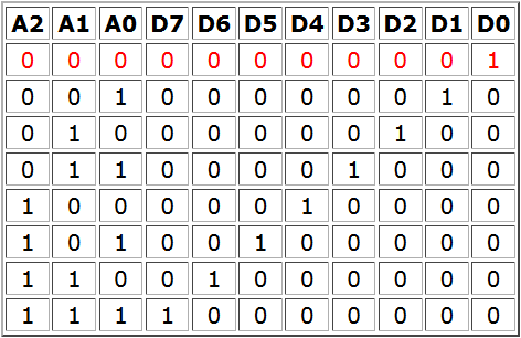
Truth table of 3 line to 8 line decoder:
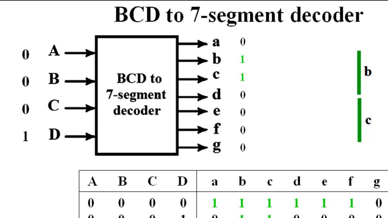
4.BCD to seven segment decoder:
It consists of a seven segment display consisting of seven light emitting diodes.The segments are denoted by letters a-g .By illuminating various combinations of segments numbers from 0-9 can be depicted.
In electronics there are two important types of 7-segment LED digital display.
5.Encoder:
1.BCD adder:
The steps followed in a BCD adder can be considered after considering the steps of BCD addition:
1.firstly the two BCD code groups are added for each decimal digit position using ordinary binary addition.
2.For those positions where the sum is 9 or less,the sum is in proper BCD format and no correction is needed.
3.When the sum of 2 digits is greater than 9 a correction of 0110 should be added to the sum,to produce proper BCD result.this will produce a carry to be added to the next decimal position.
In accordance with above rules the BCD adder performs following actions :
1.BCD adder adds the two numbers inputed and generates the output.If the sum is less than 9 then the output corresponds to the result.
2.If the sum is greater than 9(1001) then 0110 is added to the result and carry bit generated is taken to the next decimal position.

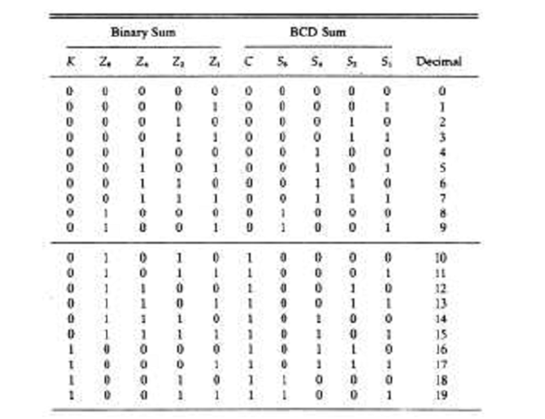
Above diagram showed us the realisation of BCD adder using two 4-bit adders and a correction detector circuit.
Only when the output carry is equal to 1 does the number 0110 be added to the binary sum to generate the new sum and carry.
2.Comparator:
A comparator is a logic circuit used to compare two binary numbers.
the X-nor gate is a basic comprator because its output is a 1 only if its two input bits are equal.
A comparator signifying which of the two numbers is greater is more complex.
if A=A3A2A1A0 and B=B3B2B1B0 be two four bit numbers then the steps followed by the comparator are:
1.Compare the most significant bits A3 and B3 of the two numbers.If A3 is a 1 and B3 is a 0 then A>B
if and only if A and B coincide go to step 2.
2.Compare the bits A2 and B2 of the numbers.if A2=1 and B2=0,A>B; if A2=0 and B2=1,A<B.if both the values coincide then goto step 3.
3.Compare the bits A1 and B1 of the numbers.If A1=1 and B1=0,A>B ;if A1=0 and B1=1,A<B if both the values coincide then goto step 4.
4..Compare the bits A0 and B0 of the numbers.If A0=1 and B0=0,A>B;if A0=0 and B0=1,A<B,if both the values coincide then A=B.


Above map shows steps for configuring a 2-bit comparator.
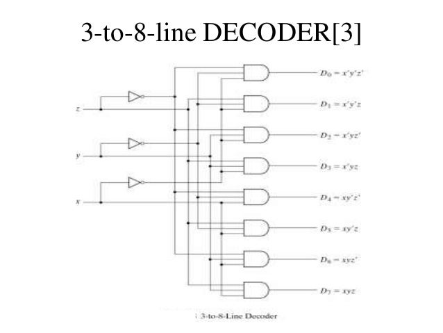
3.Decoder:
A decoder is a logic circuit that converts an N bit binary input code into M output lines such that only one output line is activated for each combination of inputs.
a 3line to 8-line decoder has 3 inputs and 8 outputs as the name suggests.For active high outputs AND gates are used and for active low outputs NAND gates are used.
Logic diagram of 3line to 8 line decoder:
An encoder has a number of input lines only one of which is activated at a given time and produces an N-bit output code depending on which input is activated.
In short it performs the reverse of the operation performed by a decoder.
Octal to binary encoder


truth table is given below:
6.Multiplexer
This logic circuit selects 1 out of several inputs and gives it as the output.

4.BCD to seven segment decoder:
It consists of a seven segment display consisting of seven light emitting diodes.The segments are denoted by letters a-g .By illuminating various combinations of segments numbers from 0-9 can be depicted.
In electronics there are two important types of 7-segment LED digital display.
- 1. The Common Cathode Display (CCD) – In the common cathode display, all the cathode connections of the LED’s are joined together to logic “0” or ground. The individual segments are illuminated by application of a “HIGH”, logic “1” signal to the individual Anode terminals.
- 2. The Common Anode Display (CAD) – In the common anode display, all the anode connections of the LED’s are joined together to logic “1” and the individual segments are illuminated by connecting the individual Cathode terminals to a “LOW”, logic “0” signal.
5.Encoder:
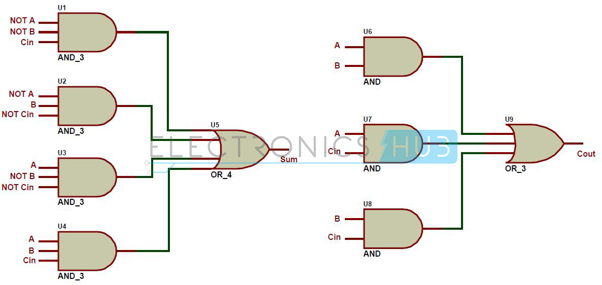
1.BCD adder:
The steps followed in a BCD adder can be considered after considering the steps of BCD addition:
1.firstly the two BCD code groups are added for each decimal digit position using ordinary binary addition.
2.For those positions where the sum is 9 or less,the sum is in proper BCD format and no correction is needed.
3.When the sum of 2 digits is greater than 9 a correction of 0110 should be added to the sum,to produce proper BCD result.this will produce a carry to be added to the next decimal position.
In accordance with above rules the BCD adder performs following actions :
1.BCD adder adds the two numbers inputed and generates the output.If the sum is less than 9 then the output corresponds to the result.
2.If the sum is greater than 9(1001) then 0110 is added to the result and carry bit generated is taken to the next decimal position.
Above diagram showed us the realisation of BCD adder using two 4-bit adders and a correction detector circuit.
Only when the output carry is equal to 1 does the number 0110 be added to the binary sum to generate the new sum and carry.
2.Comparator:
A comparator is a logic circuit used to compare two binary numbers.
the X-nor gate is a basic comprator because its output is a 1 only if its two input bits are equal.
A comparator signifying which of the two numbers is greater is more complex.
if A=A3A2A1A0 and B=B3B2B1B0 be two four bit numbers then the steps followed by the comparator are:
1.Compare the most significant bits A3 and B3 of the two numbers.If A3 is a 1 and B3 is a 0 then A>B
if and only if A and B coincide go to step 2.
2.Compare the bits A2 and B2 of the numbers.if A2=1 and B2=0,A>B; if A2=0 and B2=1,A<B.if both the values coincide then goto step 3.
3.Compare the bits A1 and B1 of the numbers.If A1=1 and B1=0,A>B ;if A1=0 and B1=1,A<B if both the values coincide then goto step 4.
4..Compare the bits A0 and B0 of the numbers.If A0=1 and B0=0,A>B;if A0=0 and B0=1,A<B,if both the values coincide then A=B.
In short it performs the reverse of the operation performed by a decoder.
Octal to binary encoder
truth table is given below:
This logic circuit selects 1 out of several inputs and gives it as the output.
| 7.Demultiplexer: | A demultiplexer has a single input line and several output lines.Depending on the select signals the output is generated. | 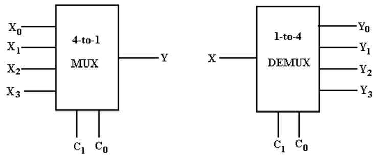 |
 |


 , subtrahend
  , and borrow in
  . The full subtractor generates two output bits: the difference
  and borrow out
  .
.
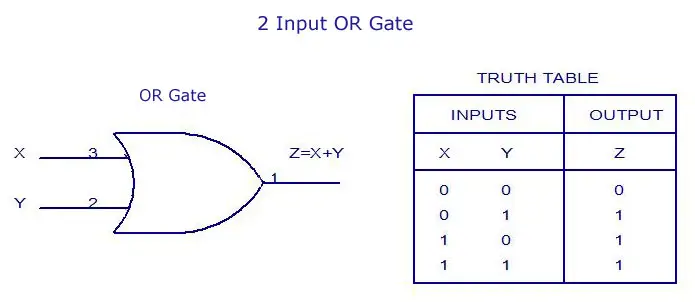 The or gate gives a low output when all its inputs are low.