Tuesday, 5 July 2016

simple diode circuits


Earlier we had discussed regarding the diode charactersitics.Diodes when connected in a particular manner can produce different waveforms across the output.We will discuss such diode configurations in this post.
          
1.AND gate using diodes

Above circuit shows an 
AND gate configured using diodes connected in parallel.When the input V is applid such that the anode is at a higher potential than the cathode the diode is forward biased giving an output .Thus the circuit gives a positive output .Even if one of the diodes is reverse biased the output is zero,since the output terminal is grounded.

2 .OR gate using diodes


Above circuit shows an OR gate configured using diodes.
Even if a single input is such that the diode in series with the source is forward biased then the output is in high state .Only when both the inputs are such that the diodes are reverse biased then the output will be zero.

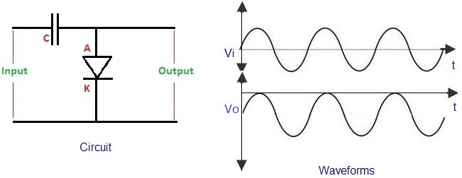
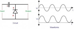
3.Half wave rectifier using diodes


The above circuit shows the configuration of half-wave rectifier using diodes.During the positive half cycle of the input waveform the diode is forward biased and it replicates the input waveform as it is .During the negative half cycle the diode is reverse biased and acts like an open circuit.Thus the output is zero for the negative half cycle of the input waveform.


4.Full wave rectifier using diodes:
If two diodes are connected such that their two cathodes and two anodes are connected back to back then the circuit acts as a full wave rectifier.During the positive half cycle diode d1 conducts while in the negative half cycle diode d2 conducts.The net voltage is the phasor sum of the two voltages and we get a steady curve across the output.

5.Bridge rectifier circuit:

Image result for full wave rectifier using diode

In bridge rectifier circuit four diodes are connected such as shown above.
During the positive half cycle of the ac input the diodes D1 ad D2 are forward biased,while in the negative half cycle diodes D3 and D4 are forward biased.Thus throughout the input cycle the output is maintained steady giving a fully rectified signal.


Sunday, 26 June 2016

Clippers and clampers

The clippers and clampers are simple diode circuits .

Clipper:
In the clipper circuit a dc source is connected in series or in parallel to the diode.As an ac input is given to the circuit,the input passes only if the diode is forward biased and the applied voltage is greater than the dc supply voltage and the dc supply is such that the voltage drop is in the direction of current flow from the ac source.For voltages of ac input less than the difference between ac input and dc input the diode is in reverse bias.Hence the diode acts as an open circuit.Thus a part of the output is clipped.


In the positive clipper the positive part of the input is clipped and in negative clipper negative part of the input is clipped.


Clampers:

Clampers are diode circuits which cause shifting of the input signal by some distance.In this circuit a capacitance is connected in series with the ac input and a diode is connected in parallel.Till the capacitance acquires potential the ac input does not pass to the diode.Thus only when the capacitance is charged the diode starts conducting.
 The capacitor must be chosen such that, during the conduction of the diode, the capacitor must be sufficient to charge quickly and during the nonconducting period of diode, the capacitor should not discharge drastically. The clampers are classified as positive and negative clampers based on the clamping method.


Negative clamper:Above figure shows a negative clamper.


Positive Clamper
Above figure shows a positive clamper.

Friday, 24 June 2016

Field effect transistors


Even though transistors were an efficient way to amplify current another device to achieve  the same came into existence.The field effect transistors were similar in operation the transistor .The basic difference between the BJT and FET is that BJT is a current controlled device whereas FET is a voltage controlled device.

The images of the bjt and fet are mentioned below:
Image result for difference between bjt and fet


There are two types of FET.They are
a.the junction field effect transistor
b.the Metal oxide semiconductor field effect transistor


Further the JFET has two types i.e
a. the n channel and
b.p channel FET.

Also the MOSFET has two types i.e
 a.the enhancement and
b.depletion type MOSFET.

 As can be seen from the diagram above the FET consists of three components i.e the source ,the drain and the gate.
    The working of  a FET can be compared to the water flowing down a tap.By controlling the tap screw the flow of water through the tap can be controlled .Similarly the gate is analogous to the tap screw,by controlling the gate voltage the flow of electrons from the source to the drain can be controlled.

http://www.circuitstoday.com/wp-content/uploads/2009/08/JFET-Junction-Field-Effect-Transistors.jpg
Characteristics of a n channel JFET:
When Vgs=0 and Vds is increased:
Since the gate voltage is zero the depletion layers are unaffected.
so the drain current increases with an increase in Drain to source voltage.


When Vgs<0 and Vds is increased:
As Vgs is very low the increase in Vds further increases the depletion layer and reaches a point called pinch-off where the drain current settles .Beyond the pinch off voltage the drain current is constant


p-Channel JFET characteristics with IDSS = 6mA and VP = +6 V.

The pinch off voltage is negative for a n channel jfet and positive for a p-channel jfet.


Types of Mosfet:
a.the enhancement type of MOSFET
Enhancement-mode MOSFETs are the common switching elements in most MOS. These devices are off at zero gate–source voltage, and can be turned on by pulling the gate voltage either higher than the source voltage, for NMOS, or lower than the source voltage, for PMOS. In most circuits, this means pulling an enhancement-mode MOSFET's gate voltage towards its drain voltage turns it ON.

The enhancement mosfet has drain characteristics similar to the 
 JFET.


b.depletion type MOSFET
In a depletion-mode MOSFET, the device is normally ON at zero gate–source voltage. Such devices are used as load "resistors" in logic circuits (in depletion-load NMOS logic, for example). For N-type depletion-load devices, the threshold voltage might be about –3 V, so it could be turned off by pulling the gate 3 V negative (the drain, by comparison, is more positive than the source in NMOS). In PMOS, the polarities are reversed.


In the N channel device, shown in Fig. 5.2 the gate is made negative with respect to the source, which has the effect of creating a depletion area, free from charge carriers, beneath the gate. This restricts the depth of the conducting channel, so increasing channel resistance and reducing current flow through the device.

N channel depletion mode MOSFET operation


Thursday, 16 June 2016

BJT -bipolar junction transistor

The invention of transistor ushered in a new era in the field of electronics.The years between 1904-1947 saw the extensive use of vacuum diode in various electronic devices.
However in the year 1947 the three scientists William shockley,John bardeen and walter bratain invented the transistor in the bell laboratories.
The transistor was not only rugged in construction and more efficient it was also smaller in size as compared to the vacuum diode.
The transistor consists of a 3 layer device having two junctions.
The transistors find extensive application in computers ,television,mobile phones,industrial areas etc and their main function is curent amplification.

The transistors can be operated in 3 configurations:
1.Common base configuration:
The emitter base junction is forward biased and base collector junction is reverse biased.
The majority carriers move from the first layer into the middle layer where they are the minority carriers.Again they are pushed into the third layer.Thus the base current is negligibly small and the emitter current is almost equivalent to the collector current.

applications:
Common base configuration is commonly used in amplifiers.

2.Common emitter configuration:

In this configuration the emitter is connected in both the input and output circuits.
the base current is the input current and the collector current acts as the output current.
the gain is given by
beta = output current / input current

The gain thus is large and hence this configuration finds wide application in amplifiers.

3.Common collector
In common collector configution the collector is common to both input and output.

it finds applications in cascaded netwrks since it does not greatly change signals.


Input characteristics of transistor in common base configuration:


Tuesday, 14 June 2016

characteristics of diodes

Ideal diode:
the ideal diode is a pn junction device which acts like a short circuit on forward bias and as open circuit when connected in reverse bias.
It acts like a switch which conducts only in one direction.
We will have a small introduction into the materials involved in making a semiconductor diodes:

Semiconductor material:
As we all know ,the various elements have 2 bands conduction band and valence band separated by energy gap.
When the electrons in the valence band are energized they jump into the conduction band if the energy supplied is sufficient to overcome the energy gap.This energy gap is given in eV or electron volt.
In conductors the valence band and conduction band almost coincide with each other.Therefore even when a small amount of energy is acquired by these they start conducting and thus they are good conductors of electrricity.
In semiconductors the energy gap is between 2eV to 5eV.Thus they are moderate conductors of electricity.
commonly used semiconductor material are silicon,germanium etc.


Extrinsic semiconductor materials:
The semiconductor material subjected to doping i.e adding of an impurity element to the semiconductor is called an extrinsic material.
The n-type materials are formed by adding a pentavalent element like phosphorus to the semiconductor.The n-type material has therefore electrons as a majority .
The p-type materials are formed by adding a trivalent element like boron to the semiconductor.The p-type material has therefore holes as a majority.

Pn junction diode:

The diode as discussed earlier is a pn junction device designed by bringing the p type and n type material together.The electrons and holes get gathered near the junction to form the depletion layer.
Diode symbol


The diode can be operated in any of the 3 ways:
1.No bias:
When no voltage is applied across the diode it acts like an open circuit.

2.Reverse bias
When the positive terminal of the voltage source is connected to the n type and the negative terinal to the p-type  material the resulting bias is reverse bias.Under reverse bias a very small reverse saturation current of minority charge carriers flows across the junction.


3.Forward bias
When the positive terminal of the voltage source is cnnected to the p type and the negative terminal to the n type the resulting bias is called forward bias.The depletion layer diminishes under the effect of forward bias as majority carriers flow across the junction and recombine.


Types of diodes:
The various diodes are illustrated below:

Image result for types of diodes symbols
We will discuss zener and photo diode in detail:
1.Zener diode:
The zener diode the direction of current flow is opposite to that in an ordinary diode.The zener diode operates in the zener region when the voltage is negative at a certain point the current shoots up considerably.since it is operated in the zener region it is called zener diode.


2.LED
It is known fact that when the diode is energised the majority carriers in the diode junction recombine and this leads to the flow of charge across the junction.The emission of light alon with this flow of charge is called electroluminescence.
GaAS (Gallium arsenide)and some other materials show this property.This property is exploited in the design of LED or light emitting diode.It emits current when connected in forward bias and indicates the flow of charge through it.

Image result for LED


Thursday, 5 May 2016

counters

A counter circuit is usually constructed of a number of flip-flops connected in cascade. Counters are a very widely-used component in digital circuits, and are manufactured as separate integrated circuits and also incorporated as parts of larger integrated circuits.

In this blog we will deal with asynchronous ,synchronous counter and ring counter:
1.Asynchronous counter:
Depending on the number of digits to be counted modulo N counters are configured.

Cycle Q1 Q0 (Q1:Q0)dec
0 0 0 0
1 0 1 1
2 1 0 2
3 1 1 3
4 0 0 0


Number of flip-flops are connected in series such that the clocks of the next flip flop is triggered by the input of previous fllip flop.
design of asynchronous counter:
1.decide the no of flip-flops from the mod number from the basic equation.
modulus n=2^n
where n is the no of flipflops.
2.connect the flip flops serially as a ripple counter
3.fimd the binary number n-1
4.connect all ff outputs that are 1 at n-1 as inputs to a NAND gate.Also feed the clock pulse to the NAND gate
5.connect the NAND gate output to the preset inputs of all the flip-flops for which Q=0 at the count n-1.


2.synchronous counters
In synchronous counters, the clock inputs of all the flip-flops are connected together and are triggered by the input pulses. Thus, all the flip-flops change state simultaneously (in parallel). The circuit below is a 4-bit synchronous counter. The J and K inputs of FF0 are connected to HIGH. FF1 has its J and K inputs connected to the output of FF0, and the J and K inputs of FF2 are connected to the output of an AND gate that is fed by the outputs of FF0 and FF1. A simple way of implementing the logic for each bit of an ascending counter (which is what is depicted in the image to the right) is for each bit to toggle when all of the less significant bits are at a logic high state. For example, bit 1 toggles when bit 0 is logic high; bit 2 toggles when both bit 1 and bit 0 are logic high; bit 3 toggles when bit 2, bit 1 and bit 0 are all high; and so on.
Synchronous counters can also be implemented with hardware finite-state machines, which are more complex but allow for smoother, more stable transitions.

 3.ring counters
A ring counter is a circular shift register which is initiated such that only one of its flip-flops is the state one while others are in their zero states.
A ring counter is a Shift Register (a cascade connection of flip-flops) with the output of the last one connected to the input of the first, that is, in a ring. Typically, a pattern consisting of a single bit is circulated so the state repeats every n clock cycles if n flip-flops are used.

Tuesday, 3 May 2016

Sequential circuits-Flip flops


Sequential circuits are circuits whose output at any instant of time depends on all previous inputs.
Flip flops are sequential circuits which are configured using a set of logic gates and they can be used as a memory element. A logic gate by itself has no storage capacity but several logic gates connected together can permit storage of data.
Flip flops are also called as bistable multivibrators.

Flip-flops can be either simple (transparent or opaque) or clocked (synchronous or edge-triggered). Although the term flip-flop has historically referred generically to both simple and clocked circuits, in modern usage it is common to reserve the term flip-flop exclusively for discussing clocked circuits; the simple ones are commonly called latches.
1 latch:


an active high  SR latch


timing diagram of a simple SR latch
2.gated latches:
gated  SR latch:

Tt is sometimes useful in logic circuits to have a multivibrator which changes state only when certain conditions are met, regardless of its S and R input states. The conditional input is called the enable, and is symbolized by the letter E. 
 

When the E=0, the outputs of the two AND gates are forced to 0, regardless of the states of either S or R. Consequently, the circuit behaves as though S and R were both 0, latching the Q and not-Q outputs in their last states. Only when the enable input is activated (1) will the latch respond to the S and R inputs

3.edge triggered flip flop:
One method of enabling a multivibrator circuit is called edge triggering, where the circuit’s data inputs have control only during the time that the enable input is transitioning from one state to another.  
edge triggered SR flip flop:

Edge-triggered S-R flip-flop


The basic operation is illustrated below, along with the truth table for this type of flip-flop. The operation and truth table for a negative edge-triggered flip-flop are the same as those for a positive except that the falling edge of the clock pulse is the triggering edge.
S-R truth table
As S = 1, R = 0.  Flip-flop SETS on the rising clock edge.
Note that the S and R inputs can be changed at any time when the clock input is LOW or HIGH (except for a very short interval around the triggering transition of the clock) without affecting the output. This is illustrated in the timing diagram below:

Edge-triggered J-K flip-flop
The J-K flip-flop works very similar to S-R flip-flop.  The only difference is that this flip-flop has NO invalid state.  The outputs toggle (change to the opposite state) when both J and K inputs are HIGH.  The truth table is shown below.
J-K truth table 
Edge-triggered D flip-flop
The operations of a D flip-flop is much more simpler.  It has only one input addition to the clock.  It is very useful when a single data bit (0 or 1) is to be stored.  If there is a HIGH on the D input when a clock pulse is applied, the flip-flop SETs and stores a 1.  If there is a LOW on the D input when a clock pulse is applied, the flip-flop RESETs and stores a 0.  The truth table below summarize the operations of the positive edge-triggered D flip-flop.  As before, the negative edge-triggered flip-flop works the same except that the falling edge of the clock pulse is the triggering edge.
D truth table


Applications of filp-flops:
Flip-flops have wide and extensive application in semiconductor memories,counters,shift and storage registers.
They can also be used for binary addition,serial decode,comparison and timing function.