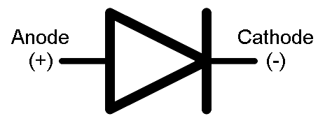
Ideal diode:
the ideal diode is a pn junction device which acts like a short circuit on forward bias and as open circuit when connected in reverse bias.
It acts like a switch which conducts only in one direction.
We will have a small introduction into the materials involved in making a semiconductor diodes:
Semiconductor material:
As we all know ,the various elements have 2 bands conduction band and valence band separated by energy gap.
When the electrons in the valence band are energized they jump into the conduction band if the energy supplied is sufficient to overcome the energy gap.This energy gap is given in eV or electron volt.
In conductors the valence band and conduction band almost coincide with each other.Therefore even when a small amount of energy is acquired by these they start conducting and thus they are good conductors of electrricity.
In semiconductors the energy gap is between 2eV to 5eV.Thus they are moderate conductors of electricity.
commonly used semiconductor material are silicon,germanium etc.

Extrinsic semiconductor materials:
The semiconductor material subjected to doping i.e adding of an impurity element to the semiconductor is called an extrinsic material.
The n-type materials are formed by adding a pentavalent element like phosphorus to the semiconductor.The n-type material has therefore electrons as a majority .
The p-type materials are formed by adding a trivalent element like boron to the semiconductor.The p-type material has therefore holes as a majority.
Pn junction diode:
The diode as discussed earlier is a pn junction device designed by bringing the p type and n type material together.The electrons and holes get gathered near the junction to form the depletion layer.
Diode symbol

The diode can be operated in any of the 3 ways:
1.No bias:
When no voltage is applied across the diode it acts like an open circuit.
2.Reverse bias
When the positive terminal of the voltage source is connected to the n type and the negative terinal to the p-type material the resulting bias is reverse bias.Under reverse bias a very small reverse saturation current of minority charge carriers flows across the junction.

3.Forward bias
When the positive terminal of the voltage source is cnnected to the p type and the negative terminal to the n type the resulting bias is called forward bias.The depletion layer diminishes under the effect of forward bias as majority carriers flow across the junction and recombine.

Types of diodes:
The various diodes are illustrated below:

We will discuss zener and photo diode in detail:
1.Zener diode:
The zener diode the direction of current flow is opposite to that in an ordinary diode.The zener diode operates in the zener region when the voltage is negative at a certain point the current shoots up considerably.since it is operated in the zener region it is called zener diode.

2.LED
It is known fact that when the diode is energised the majority carriers in the diode junction recombine and this leads to the flow of charge across the junction.The emission of light alon with this flow of charge is called electroluminescence.
GaAS (Gallium arsenide)and some other materials show this property.This property is exploited in the design of LED or light emitting diode.It emits current when connected in forward bias and indicates the flow of charge through it.


the ideal diode is a pn junction device which acts like a short circuit on forward bias and as open circuit when connected in reverse bias.
It acts like a switch which conducts only in one direction.
We will have a small introduction into the materials involved in making a semiconductor diodes:
Semiconductor material:
As we all know ,the various elements have 2 bands conduction band and valence band separated by energy gap.
When the electrons in the valence band are energized they jump into the conduction band if the energy supplied is sufficient to overcome the energy gap.This energy gap is given in eV or electron volt.
In conductors the valence band and conduction band almost coincide with each other.Therefore even when a small amount of energy is acquired by these they start conducting and thus they are good conductors of electrricity.
In semiconductors the energy gap is between 2eV to 5eV.Thus they are moderate conductors of electricity.
commonly used semiconductor material are silicon,germanium etc.
Extrinsic semiconductor materials:
The semiconductor material subjected to doping i.e adding of an impurity element to the semiconductor is called an extrinsic material.
The n-type materials are formed by adding a pentavalent element like phosphorus to the semiconductor.The n-type material has therefore electrons as a majority .
The p-type materials are formed by adding a trivalent element like boron to the semiconductor.The p-type material has therefore holes as a majority.
Pn junction diode:
The diode as discussed earlier is a pn junction device designed by bringing the p type and n type material together.The electrons and holes get gathered near the junction to form the depletion layer.
Diode symbol

The diode can be operated in any of the 3 ways:
1.No bias:
When no voltage is applied across the diode it acts like an open circuit.
2.Reverse bias
When the positive terminal of the voltage source is connected to the n type and the negative terinal to the p-type material the resulting bias is reverse bias.Under reverse bias a very small reverse saturation current of minority charge carriers flows across the junction.
3.Forward bias
When the positive terminal of the voltage source is cnnected to the p type and the negative terminal to the n type the resulting bias is called forward bias.The depletion layer diminishes under the effect of forward bias as majority carriers flow across the junction and recombine.
Types of diodes:
The various diodes are illustrated below:
We will discuss zener and photo diode in detail:
1.Zener diode:
The zener diode the direction of current flow is opposite to that in an ordinary diode.The zener diode operates in the zener region when the voltage is negative at a certain point the current shoots up considerably.since it is operated in the zener region it is called zener diode.
2.LED
It is known fact that when the diode is energised the majority carriers in the diode junction recombine and this leads to the flow of charge across the junction.The emission of light alon with this flow of charge is called electroluminescence.
GaAS (Gallium arsenide)and some other materials show this property.This property is exploited in the design of LED or light emitting diode.It emits current when connected in forward bias and indicates the flow of charge through it.
No comments:
Post a Comment