Sunday 26 June 2016

Clippers and clampers

The clippers and clampers are simple diode circuits .

Clipper:
In the clipper circuit a dc source is connected in series or in parallel to the diode.As an ac input is given to the circuit,the input passes only if the diode is forward biased and the applied voltage is greater than the dc supply voltage and the dc supply is such that the voltage drop is in the direction of current flow from the ac source.For voltages of ac input less than the difference between ac input and dc input the diode is in reverse bias.Hence the diode acts as an open circuit.Thus a part of the output is clipped.


In the positive clipper the positive part of the input is clipped and in negative clipper negative part of the input is clipped.


Clampers:

Clampers are diode circuits which cause shifting of the input signal by some distance.In this circuit a capacitance is connected in series with the ac input and a diode is connected in parallel.Till the capacitance acquires potential the ac input does not pass to the diode.Thus only when the capacitance is charged the diode starts conducting.
 The capacitor must be chosen such that, during the conduction of the diode, the capacitor must be sufficient to charge quickly and during the nonconducting period of diode, the capacitor should not discharge drastically. The clampers are classified as positive and negative clampers based on the clamping method.


Negative clamper:Above figure shows a negative clamper.


Positive Clamper
Above figure shows a positive clamper.

Friday 24 June 2016

Field effect transistors


Even though transistors were an efficient way to amplify current another device to achieve  the same came into existence.The field effect transistors were similar in operation the transistor .The basic difference between the BJT and FET is that BJT is a current controlled device whereas FET is a voltage controlled device.

The images of the bjt and fet are mentioned below:
Image result for difference between bjt and fet


There are two types of FET.They are
a.the junction field effect transistor
b.the Metal oxide semiconductor field effect transistor


Further the JFET has two types i.e
a. the n channel and
b.p channel FET.

Also the MOSFET has two types i.e
 a.the enhancement and
b.depletion type MOSFET.

 As can be seen from the diagram above the FET consists of three components i.e the source ,the drain and the gate.
    The working of  a FET can be compared to the water flowing down a tap.By controlling the tap screw the flow of water through the tap can be controlled .Similarly the gate is analogous to the tap screw,by controlling the gate voltage the flow of electrons from the source to the drain can be controlled.

http://www.circuitstoday.com/wp-content/uploads/2009/08/JFET-Junction-Field-Effect-Transistors.jpg
Characteristics of a n channel JFET:
When Vgs=0 and Vds is increased:
Since the gate voltage is zero the depletion layers are unaffected.
so the drain current increases with an increase in Drain to source voltage.


When Vgs<0 and Vds is increased:
As Vgs is very low the increase in Vds further increases the depletion layer and reaches a point called pinch-off where the drain current settles .Beyond the pinch off voltage the drain current is constant


p-Channel JFET characteristics with IDSS = 6mA and VP = +6 V.

The pinch off voltage is negative for a n channel jfet and positive for a p-channel jfet.


Types of Mosfet:
a.the enhancement type of MOSFET
Enhancement-mode MOSFETs are the common switching elements in most MOS. These devices are off at zero gate–source voltage, and can be turned on by pulling the gate voltage either higher than the source voltage, for NMOS, or lower than the source voltage, for PMOS. In most circuits, this means pulling an enhancement-mode MOSFET's gate voltage towards its drain voltage turns it ON.

The enhancement mosfet has drain characteristics similar to the 
 JFET.


b.depletion type MOSFET
In a depletion-mode MOSFET, the device is normally ON at zero gate–source voltage. Such devices are used as load "resistors" in logic circuits (in depletion-load NMOS logic, for example). For N-type depletion-load devices, the threshold voltage might be about –3 V, so it could be turned off by pulling the gate 3 V negative (the drain, by comparison, is more positive than the source in NMOS). In PMOS, the polarities are reversed.


In the N channel device, shown in Fig. 5.2 the gate is made negative with respect to the source, which has the effect of creating a depletion area, free from charge carriers, beneath the gate. This restricts the depth of the conducting channel, so increasing channel resistance and reducing current flow through the device.

N channel depletion mode MOSFET operation


Thursday 16 June 2016

BJT -bipolar junction transistor

The invention of transistor ushered in a new era in the field of electronics.The years between 1904-1947 saw the extensive use of vacuum diode in various electronic devices.
However in the year 1947 the three scientists William shockley,John bardeen and walter bratain invented the transistor in the bell laboratories.
The transistor was not only rugged in construction and more efficient it was also smaller in size as compared to the vacuum diode.
The transistor consists of a 3 layer device having two junctions.
The transistors find extensive application in computers ,television,mobile phones,industrial areas etc and their main function is curent amplification.

The transistors can be operated in 3 configurations:
1.Common base configuration:
The emitter base junction is forward biased and base collector junction is reverse biased.
The majority carriers move from the first layer into the middle layer where they are the minority carriers.Again they are pushed into the third layer.Thus the base current is negligibly small and the emitter current is almost equivalent to the collector current.

applications:
Common base configuration is commonly used in amplifiers.

2.Common emitter configuration:

In this configuration the emitter is connected in both the input and output circuits.
the base current is the input current and the collector current acts as the output current.
the gain is given by
beta = output current / input current

The gain thus is large and hence this configuration finds wide application in amplifiers.

3.Common collector
In common collector configution the collector is common to both input and output.

it finds applications in cascaded netwrks since it does not greatly change signals.


Input characteristics of transistor in common base configuration:


Tuesday 14 June 2016

characteristics of diodes

Ideal diode:
the ideal diode is a pn junction device which acts like a short circuit on forward bias and as open circuit when connected in reverse bias.
It acts like a switch which conducts only in one direction.
We will have a small introduction into the materials involved in making a semiconductor diodes:

Semiconductor material:
As we all know ,the various elements have 2 bands conduction band and valence band separated by energy gap.
When the electrons in the valence band are energized they jump into the conduction band if the energy supplied is sufficient to overcome the energy gap.This energy gap is given in eV or electron volt.
In conductors the valence band and conduction band almost coincide with each other.Therefore even when a small amount of energy is acquired by these they start conducting and thus they are good conductors of electrricity.
In semiconductors the energy gap is between 2eV to 5eV.Thus they are moderate conductors of electricity.
commonly used semiconductor material are silicon,germanium etc.


Extrinsic semiconductor materials:
The semiconductor material subjected to doping i.e adding of an impurity element to the semiconductor is called an extrinsic material.
The n-type materials are formed by adding a pentavalent element like phosphorus to the semiconductor.The n-type material has therefore electrons as a majority .
The p-type materials are formed by adding a trivalent element like boron to the semiconductor.The p-type material has therefore holes as a majority.

Pn junction diode:

The diode as discussed earlier is a pn junction device designed by bringing the p type and n type material together.The electrons and holes get gathered near the junction to form the depletion layer.
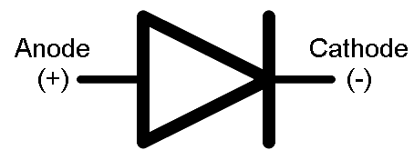
Diode symbol


The diode can be operated in any of the 3 ways:
1.No bias:
When no voltage is applied across the diode it acts like an open circuit.

2.Reverse bias
When the positive terminal of the voltage source is connected to the n type and the negative terinal to the p-type  material the resulting bias is reverse bias.Under reverse bias a very small reverse saturation current of minority charge carriers flows across the junction.


3.Forward bias
When the positive terminal of the voltage source is cnnected to the p type and the negative terminal to the n type the resulting bias is called forward bias.The depletion layer diminishes under the effect of forward bias as majority carriers flow across the junction and recombine.


Types of diodes:
The various diodes are illustrated below:

Image result for types of diodes symbols
We will discuss zener and photo diode in detail:
1.Zener diode:
The zener diode the direction of current flow is opposite to that in an ordinary diode.The zener diode operates in the zener region when the voltage is negative at a certain point the current shoots up considerably.since it is operated in the zener region it is called zener diode.


2.LED
It is known fact that when the diode is energised the majority carriers in the diode junction recombine and this leads to the flow of charge across the junction.The emission of light alon with this flow of charge is called electroluminescence.
GaAS (Gallium arsenide)and some other materials show this property.This property is exploited in the design of LED or light emitting diode.It emits current when connected in forward bias and indicates the flow of charge through it.

Image result for LED