Friday, 19 August 2016

feedback amplifiers

The connection circuit in a closed loop such that a portion of the output is fed back to the input is called a feedback network.The feedback in which the output when applied to the input diminishes the output is called as negative feedback.


A feedback amplifier therefore may be positive feedback or negative feedback depending on whether the output when fed back to the input enhances or decreases the output.

Classification of feedback amplifier :\

1.Voltage amplifiers:\
The voltage amplifiers have voltage output proportional to the input voltage signal and the proportionality factor is irrespective of the input source resistance and load resistance.

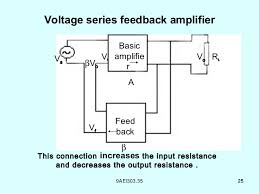
Voltage series amplifier has input terminals across a voltage source and output is drawn across the load resistance.


2. Current series feedback:
The output voltage is directly proportional to the input currenthe proportionality factor is irrespective of the source and load resistances.


3.Voltage shunt feedback:
The output cuurent is directly proportional to the input voltage.


4.Current shunt feedback:
The input and output current are in direct proprtion and the proptionality factor is independent of Rs and Rl.


An important table is given below:


Monday, 8 August 2016

frequency response of the transistor

The transistor symbol and characteristics have been discussed in a previous post.The transistor behaviour is different under low frequency and high frequency conditions.The transistor has two capacitances Cbe and Cbc between the base emitter and the base collector terminals.
1.Under low frequency conditions the reactance is high because of the low values of capacitance and frequency both.So it can be considered as open circuit.
2.On the other hand under high frequency conditions the capacitance and frequency values cause a considerable reactance,leading to a voltage divider configuration.Hence the gain of the circuit is impacted.

For low frequency analysis the two port equivalent circuit is used.

The h parameters are used to relate the voltage and current in output and input of a transistor. 
 v1=h11*i1+h12*v2
i2=h21*i1+h22*v2

h11=(v1/i1)at v2=0{input resistance at output short circuit}
h12=(v1/v2)at i1=0{reverse transfer ratio}
h21=(i2/i1) at v2=0{forward transfer ratio}
h22=(i2/v2)at  i1=0 {output conductance at input open circuit }

The transistor equivalent circuit at low frequency is as below:
 

The transistor model at high frquencies is shown below:


The Miller effect occurs only in inverting amplifiers –it
is the inverting gain that
magnifies the feedback capacitance.
 
Hi

Sunday, 24 July 2016

jfet-Biasing


Difference between jfet and bjt:

  • Jfet is mostly used in switching operations while bjt is used for linear circuits.
  • The voltage gain does not hold good for the fet ,however a bjt gives a fixed voltage gain depending on the configurtion.
  • As we all know bjt is a current controlled device whereas fet is a voltage controlled device.The biasing methods of a fet are similr to those discussed in bjt biasing techniques.

Let us get to know them:

1.fixed bias:

The figure below shows the fixed bias configuration for a n type JFET. The circuit used for its dc analysis is shown below.
Applying KVL in the gate to source loop;
-Vgs-Vgg=0
therefore,Vgs=(-Vgg).

Since Vgg is having fixed value Vgs is also having a fixed value and hence the configuration is called as fixed bias.

The drain current Id can be calculated from shockley's equation:

Id=Idss(1-(Vgs/Vp))^2.
The other parameters can be also calculated as:
Vd=Vdd-Id*Rd.

Vgs=Vg-Vs.

and since source is grounded Vs=0.
Hence
Vgs=Vg.

also
Vds=Vd.


2.self bias:

The self bias configuration eliminates the need for two dc supplies.The controlling gate to source voltage is determined by resistor in the source leg.


Vrs=Id*Rs
since Id=Is
Using KVL
-Vgs-Vrs=0
Vgs=-Vrs


Also Id=Idss(1-(Vgs/Vp))^2
On substituting Vgs and solving further we get quadratic equation:
Id^2+K1*Id+K2=0.

which can be solved to find Id.


vds=vdd-Is*RD-Is*Rs
since Id=Is.

3.Voltage divider bias:

The voltage divider biasing configuration is similar to the network we had seen in transistor biasing.
The gate  voltage is dependent on both the resistor R2 and R1 in the network.


Vg=Vdd*(R2/(R2+R1))

Id=(Vg-Vgs)/Rs

Vds=Vdd-Id*Rd-Id*Rs

Since Id=Is.


Sunday, 17 July 2016

biasing of the bjt (part 2)

 We Have discussed two varieties of bias connections.we will consider few more bias connections in this post.
a.emitter bias:


In emitter bias configuration the input is applied across the base and the emitter and the output
is taken across the collector and emitter.
Ib=(vee-0.7)/rb+(h+1) re
Ic=h* Ib
Ie=(h+1) Ib
Vce=vcc-Ic*(rc+re)

B.collector feedback bias:
This configuration employs negative feedback to prevent thermal runaway and stabilize the operating point. In this form of biasing, the base resistor  is connected to the collector instead of connecting it to the DC source . So any thermal runaway will induce a voltage drop across the  resistor that will throttle the transistor's base current.


Vcc=(Ic+Ib) Rc+Ib*Rb+vbe
Ib=(Vcc-vbe)/Rb+(h+1) Rc
Ic=h*Ib
Vce=Vcc-Ic*Rc

C.emitter feed back bias:

The fixed bias circuit is modified by attaching an external resistor to the emitter. This resistor introduces negative feedback that stabilizes the Q-point.
The way feedback controls the bias point is as follows. If Vbe is held constant and temperature increases, emitter current increases. However, a larger Ie increases the emitter voltage Ve = IeRe, which in turn reduces the voltage VRb across the base resistor. A lower base-resistor voltage drop reduces the base current, which results in less collector current because Ic = β IB. Collector current and emitter current are related by Ic = α Ie with α ≈ 1, so the increase in emitter current with temperature is opposed, and the operating point is kept stable.


Ib=(Vcc-vbe)/(rb+(h+1) re)
Ic=h*Ib
Ie=(h+1)*Ib
Vce=Vcc-(Ic*Rc)-(Ic*Re)


Monday, 11 July 2016

Biasing of the BJT

The transistors and their configurations have been discussed in our previous post.
So let us discuss the two frequently used biasing techniques in this post.

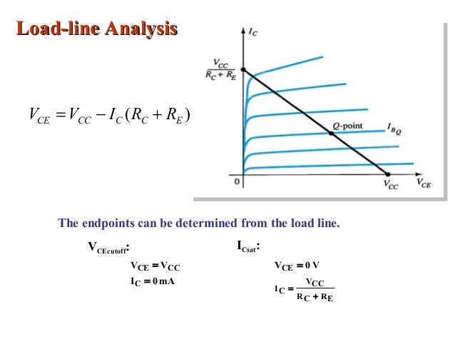
Before we get into the details of the above mentioned techniques,it is important to get an understanding of Q point or quiscient point.If we plot the Vc vs Ic curve we get the load characteristics of the BJT.On the other hand the plot of Ic for different values of Ib is taken.The intersection of these plots gives the Q point.
This analysis is called as load line analysis.


Fixed bias:
When the transistor is connected in fixed bias,the base is common to both input and output and a fixed dc supply is given to the collector and base.
Fixed Bias or Base Bias. In this condition a single power source is applied to the collector and base of the transistor using only two resistors. Applying KVL to the circuit, Thus, by merely changing the value of the resistor the base current can be adjusted to the desired value
The various equations which can be derived for this bias are as below:

Ib=(Vcc-Vbe)/Rb

Ie=Ve/Re

Ic =h Ib

where h is the ac gain.


Voltage divider circuit:


Equations governing this bias are:

Vb=Vcc*R2/((R1)+R2))
Ve=Vb-0.7
Ie=Ve/Re
Ic can be approxiately taken to be equal to Ie.
Ib=Ie/(h+1)
where h is ac gain
Vce=Vcc-Ic(Rc+Re)

Tuesday, 5 July 2016

simple diode circuits


Earlier we had discussed regarding the diode charactersitics.Diodes when connected in a particular manner can produce different waveforms across the output.We will discuss such diode configurations in this post.
          
1.AND gate using diodes

Above circuit shows an 
AND gate configured using diodes connected in parallel.When the input V is applid such that the anode is at a higher potential than the cathode the diode is forward biased giving an output .Thus the circuit gives a positive output .Even if one of the diodes is reverse biased the output is zero,since the output terminal is grounded.

2 .OR gate using diodes


Above circuit shows an OR gate configured using diodes.
Even if a single input is such that the diode in series with the source is forward biased then the output is in high state .Only when both the inputs are such that the diodes are reverse biased then the output will be zero.

3.Half wave rectifier using diodes


The above circuit shows the configuration of half-wave rectifier using diodes.During the positive half cycle of the input waveform the diode is forward biased and it replicates the input waveform as it is .During the negative half cycle the diode is reverse biased and acts like an open circuit.Thus the output is zero for the negative half cycle of the input waveform.


4.Full wave rectifier using diodes:
If two diodes are connected such that their two cathodes and two anodes are connected back to back then the circuit acts as a full wave rectifier.During the positive half cycle diode d1 conducts while in the negative half cycle diode d2 conducts.The net voltage is the phasor sum of the two voltages and we get a steady curve across the output.

5.Bridge rectifier circuit:

Image result for full wave rectifier using diode

In bridge rectifier circuit four diodes are connected such as shown above.
During the positive half cycle of the ac input the diodes D1 ad D2 are forward biased,while in the negative half cycle diodes D3 and D4 are forward biased.Thus throughout the input cycle the output is maintained steady giving a fully rectified signal.


Sunday, 26 June 2016

Clippers and clampers

The clippers and clampers are simple diode circuits .

Clipper:
In the clipper circuit a dc source is connected in series or in parallel to the diode.As an ac input is given to the circuit,the input passes only if the diode is forward biased and the applied voltage is greater than the dc supply voltage and the dc supply is such that the voltage drop is in the direction of current flow from the ac source.For voltages of ac input less than the difference between ac input and dc input the diode is in reverse bias.Hence the diode acts as an open circuit.Thus a part of the output is clipped.


In the positive clipper the positive part of the input is clipped and in negative clipper negative part of the input is clipped.


Clampers:

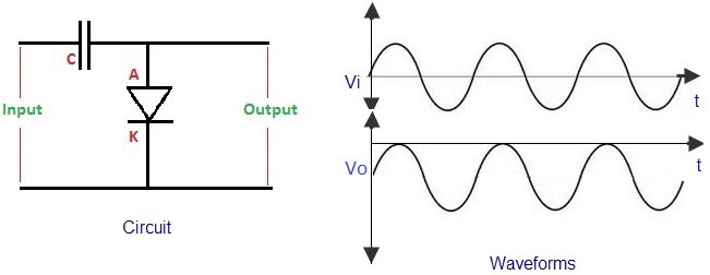
Clampers are diode circuits which cause shifting of the input signal by some distance.In this circuit a capacitance is connected in series with the ac input and a diode is connected in parallel.Till the capacitance acquires potential the ac input does not pass to the diode.Thus only when the capacitance is charged the diode starts conducting.
 The capacitor must be chosen such that, during the conduction of the diode, the capacitor must be sufficient to charge quickly and during the nonconducting period of diode, the capacitor should not discharge drastically. The clampers are classified as positive and negative clampers based on the clamping method.


Negative clamper:Above figure shows a negative clamper.


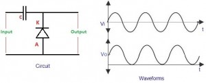
Positive Clamper
Above figure shows a positive clamper.